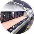
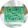
PCB Manufacturing Capability:
|
Article |
Description |
Capability |
|
|
Sercive |
PCB and SMT assembly with one-stop service |
||
|
Material |
Laminate materials |
FR4, high TG FR4, high frequency, alum, FPC |
|
|
Board cutting |
Number of layers |
1-48 |
|
|
Min.thickness for inner layers (Cu thickness are excluded) |
0.003”(0.07mm) |
||
|
Board thickness |
Standard |
(0.1-4mm±10%) |
|
|
Min. |
Single/Double:0.008±0.004” |
||
|
4layer:0.01±0.008” |
|||
|
8layer:0.01±0.008” |
|||
|
Bow and twist |
no more than 7/1000 |
||
|
Copper weight |
Outer Cu weight |
0.5-4 0z |
|
|
Inner Cu weight |
0.5-3 0z |
||
|
Drilling |
Min size |
0.0078”(0.2mm) |
|
|
Drill deviation |
±0.002″(0.05mm) |
||
|
PTH hole tolerance |
±0.002″(0.005mm) |
||
|
NPTH hole tolerance |
±0.002″(0.005mm) |
||
|
Solder mask
|
Color |
Green,white,black,red,blue… |
|
|
Min solder mask clearanace |
0.003″(0.07mm) |
||
|
Thickness |
(0.012*0.017mm) |
||
|
Silkscreen |
Color |
white,black,yellow,blue… |
|
|
Min size |
0.006″(0.15mm) |
||
|
E-test |
Function Test |
100% Functional test |
|
|
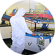
PCBA Testing |
X-ray,AOI Test,Functional test |
||
|
Pcb assembly |
one-stop service electronic manufacxturer service |
||
|
Component sourcing |
Yes |
||
|
Certificate |
IATF16949, ISO13485, ISO9001 |
||
|
Delivery time: |
PCB |
3-8days |
|
|
PCBA |
10-20days |
||
|
Tolerance of pcb |
±5% |
||
|
Max size of finish board |
700*460mm |
||
|
MOQ |
NO MOQ (1pcs) |
||
|
Surface Finish |
HASL,ENIG,immersion silver,immersion tin,OSP… |
||
|
PCB outline |
Square,circle,irregular(with jigs) |
||
|
package |
QFN,BGA,SSOP,PLCC,LGA |
||
|
Sub-assembly |
Plastic,metal,screen |
||
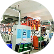
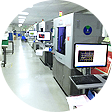
PCB MANUFACTURING PROCESSES

-step 1-
Customer data pre-review

-Step 2-
Sales quotation

-Step 3-
Engineering data production
-Step 4-
Cutting, drilling
-Step 5-
Graphics transfer
-Step 6-
Electroplating, etching
-Step 7-
Solder mask, text
-Step 8-
Surface treatment process
-Step 9-
Forming
-Step 10-
Inspection

-Step 11-
Shipment

-Step 12-
Service